


Products
Copper Substrate Wafer Scribing
 |
ProductName
Copper Substrate Wafer Scribing
Model:
Categories: Metal/Alloys

Contact NowClick here to send inquiry
Description:
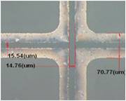
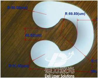
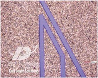
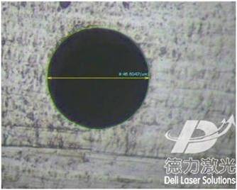
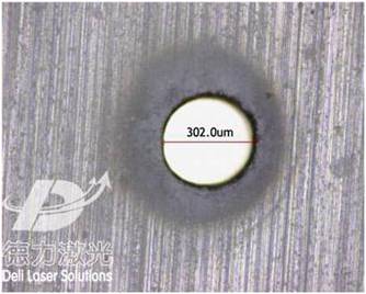
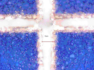
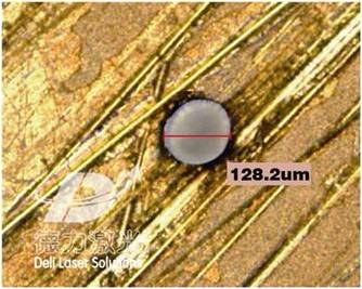
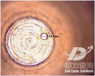
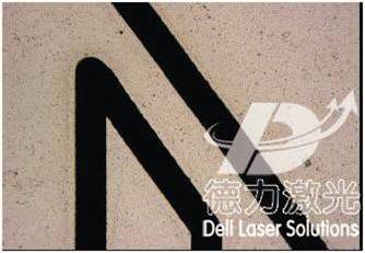
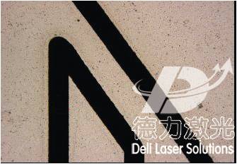
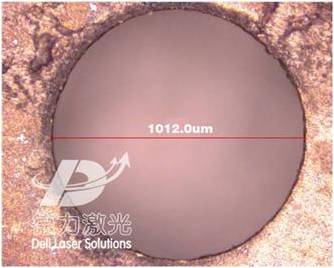
?Description:Laser scribing of COPPER substrate wafer
Scribing width: 15um, Min scribing width: 6um
Description:High accuracy and very small tolerance
-Eliminating the time-consuming and costly tool fabrication stage
Increasing the goods supply efficiency by a big margin and shortening processing circle
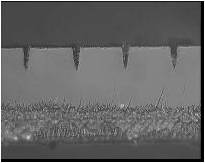
The wafer micro-cracks and the micro-crack propagation greatly reduced by Laser scribing, also the LED monomer closer. Compare with traditional way, laser scribing not only improve the production efficiency but also increased the production capacity and the processing speed. Meanwhile ,the laser scribing avoid the processing defects.
Previous Product:laser doping
Next Product:Molybdenum drilling and Molybdenum cutting
Reference


